Almae Technologies is a young company specialized in wafer growth and wafer processing of III-V compound semiconductor materials (InGaAsP and AlInGaAs alloys on InP substrate) key technologies to make advanced photonic components (photonic circuits based on laser, modulator, amplifier, waveguide integrated on the same InP wafer). Almae Technologies masters all key building blocks from design of heterostructures to testing of advanced optoelectronic functions at chip level, including all manufacturing steps : epitaxy growth and regrowth and wafer fabrication using micro and nano-scale advanced processes.
 Heterostructure and Laser architecture design
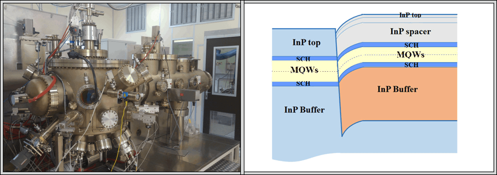 Passive Active Integration
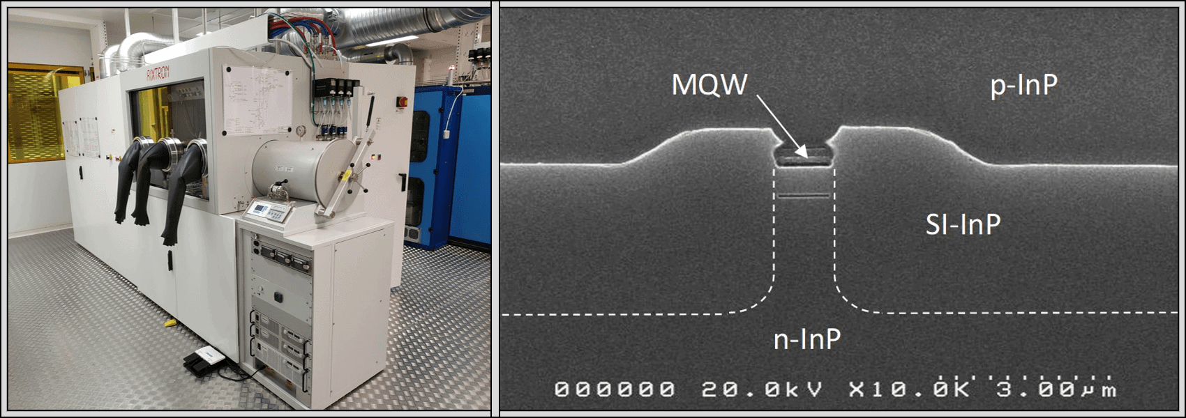 Semi Insulating Buried Heterostructure (SIBH) Technology
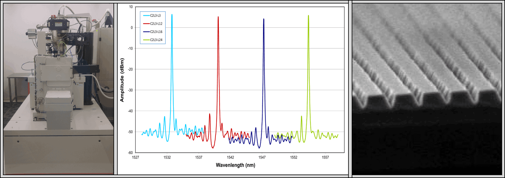 Nanolithography
 InP wafer processing platform
 Back-End
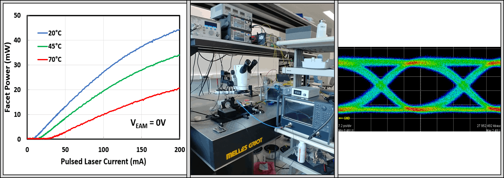 Electro-Optic devices characterizations
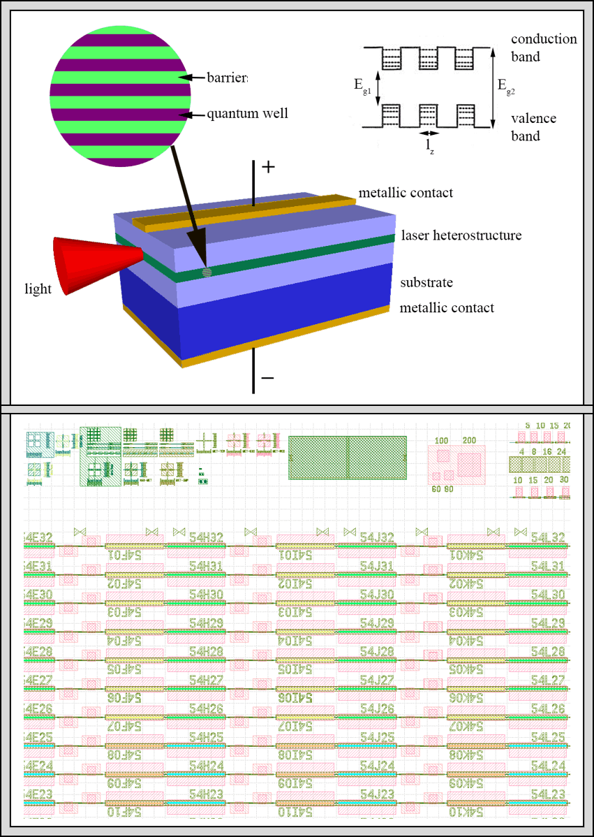 Heterostructure and Laser architecture design
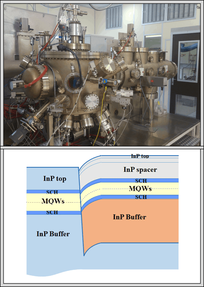 Passive Active Integration
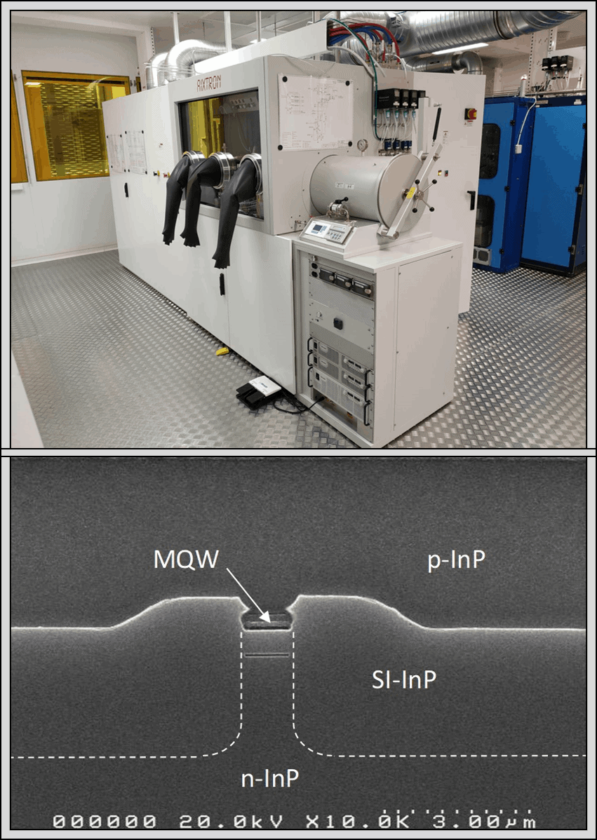 Semi Insulating Buried Heterostructure (SIBH) Technology
 Nanolithography
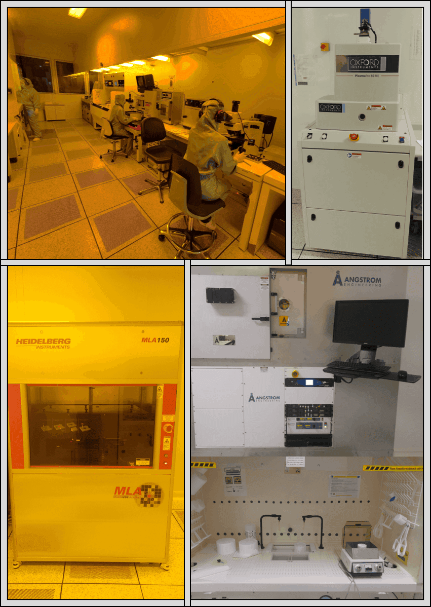 InP wafer processing platform
 Back-End
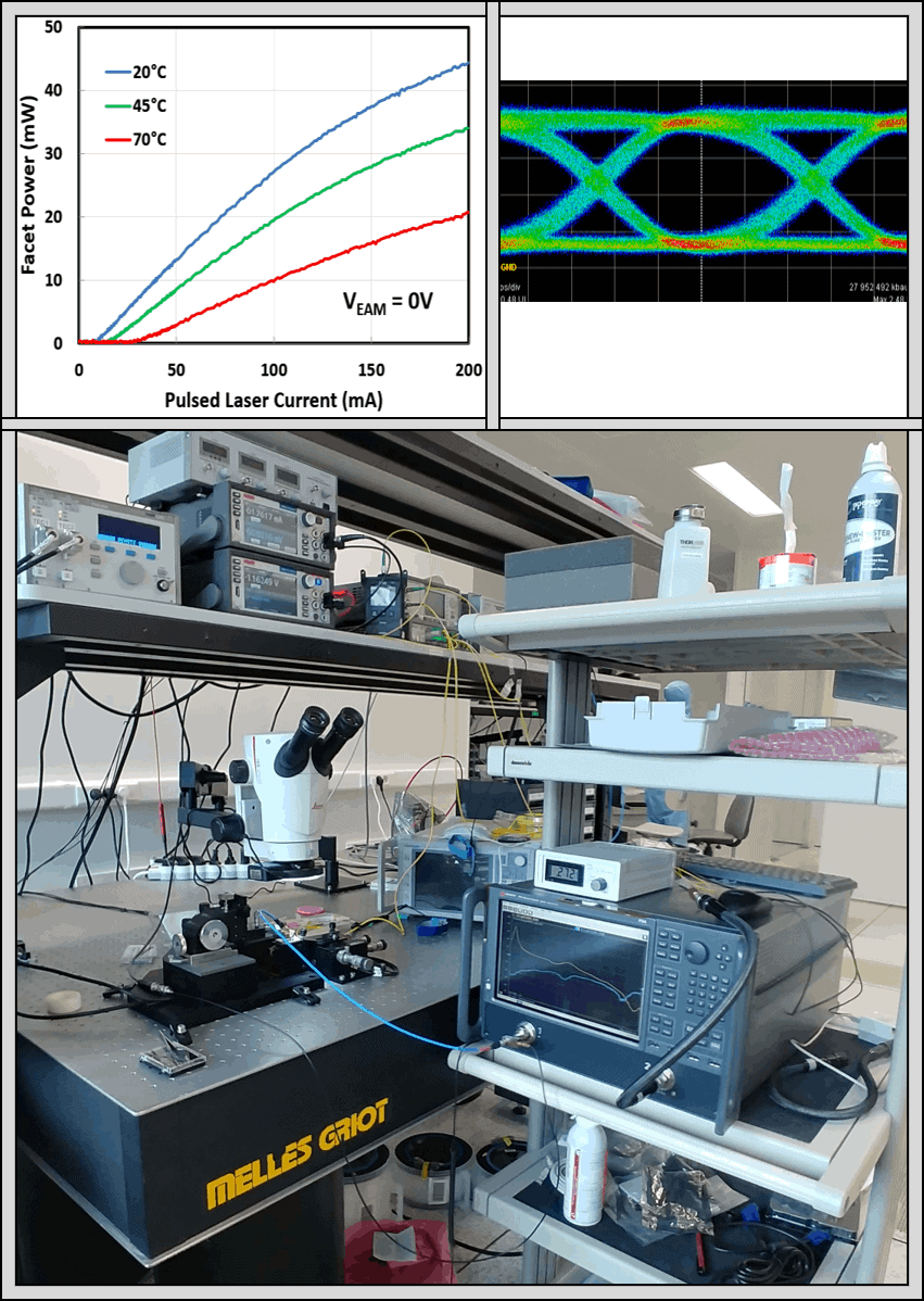 Electro-Optic devices characterizations
An overview of our technology with a focus on high power DFB lasers: