 ProductsProducts
 ServicesServices
 Publications
 News
News About UsAbout Us
 TechnologyTechnology
Our Innovation at your service
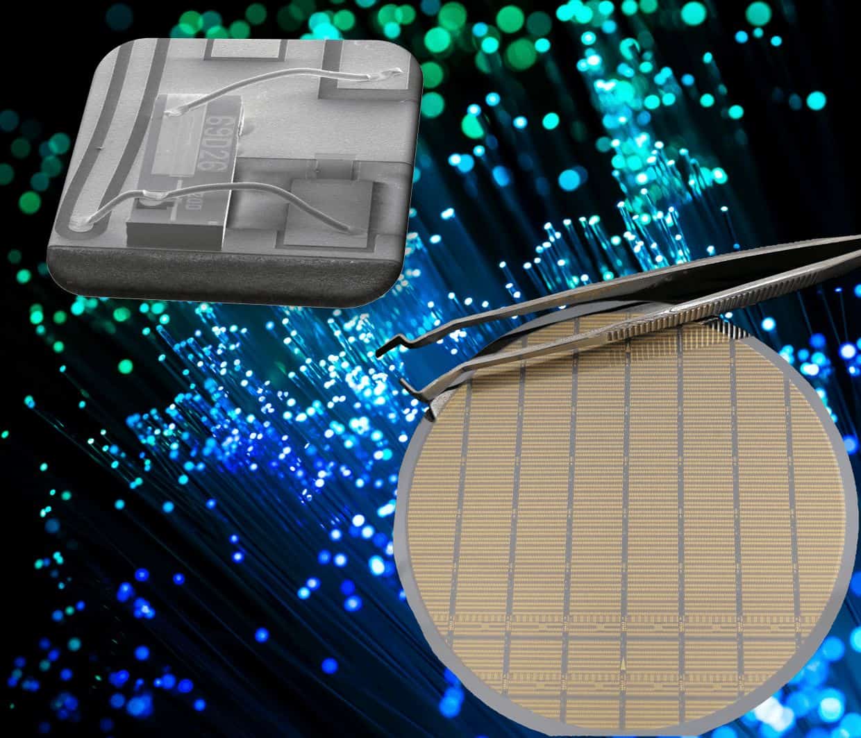
Next generation photonic chips supplier
Our Innovation at your service
Next generation photonic chips supplier
Next generation photonic chips supplier
Next generation photonic chips supplier
ProductsProductsServicesServicesPublicationsNewsAbout UsAbout UsTechnologyTechnology