Almae designs and manufactures InP based ultra-high speed integrated photonic chips which are essential to next generation telecom and datacom infrastructures, and more broadly to all future connectivity solutions.
Almae’s buried heterostructure laser technology offers a seamless solution to scale transmission speed from 10G to more than 100Gb/s. Benefits of our technology are found in lower chip to fiber or waveguide coupling losses, thanks to easy to integrate spot size converter, lower thermal resistance enabling high temperature operation, smallest size modulator and intrinsic low capacitance to give the best overall performance.
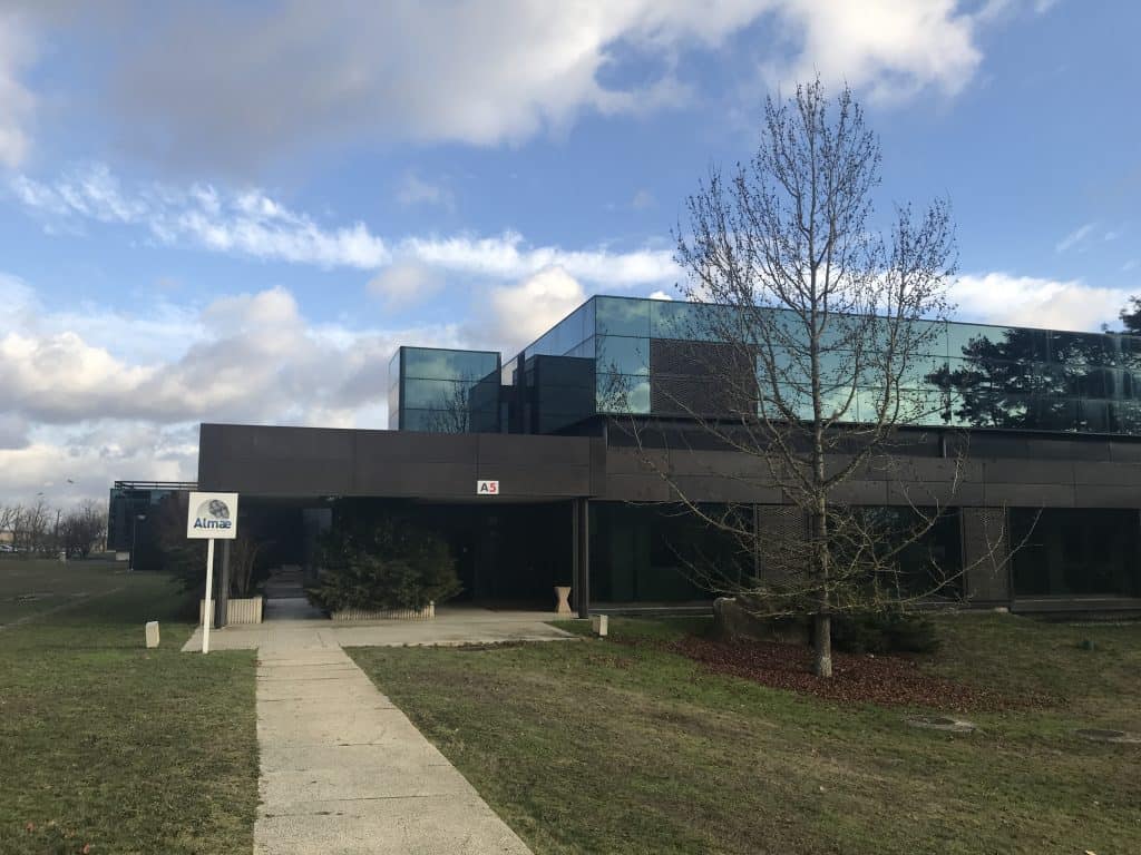
With 2000 m² of clean room and a complete set of production tools, Almae Technologies has an annual production capacity of more than one thousand 3” or 4” InP wafers. Wafer fab organization enables a quick wafer turnaround time for new product development and a straightforward and seamless transfer to production. Almae premises are located in Marcoussis, France, south of Paris in the heart of the Paris-Saclay high-tech campus.
