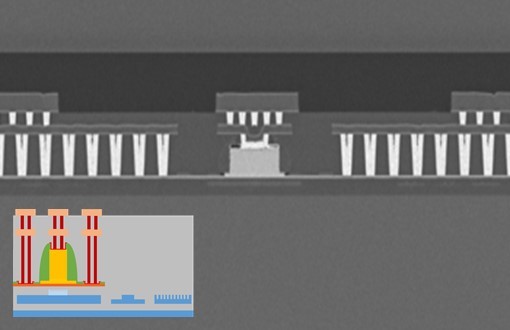
In this paper, we present the hybrid III-V/Si photonic platform developed in CEA-LETI. The overall integration is done in a fully CMOS compatible 200-mm technology, scalable to 300-mm wafers, leveraging the large-scale integration capabilities of silicon photonics. III-V material is integrated on top of a mature silicon photonic front-end wafer through direct molecular bonding enabling the monolithic integration of light sources. DFB and distributed Bragg reflector (DBR) laser reference designs are used as test vehicles for the process validation. A modular approach is used in order to minimize the impact on the already qualified silicon-based devices. Collective III-V die bonding is proposed in this platform. CMOS compatible metallizations are used to form ohmic contact on n-InP and P-InGaAs leading to contact resistivity in the range of 10 -6 Ω·cm 2 . A planarized two-metal-level BEOL is used to connect the device, leading to a drastic reduction of series resistance. Finally, the functionality of both types of lasers is demonstrated with SMSR up to 50 dB and maximum output power of 5 mW.
Published in: IEEE Journal of Selected Topics in Quantum Electronics ( Volume: 25 , Issue: 5 , Sept.-Oct. 2019 )